- 您现在的位置:买卖IC网 > Sheet目录2001 > ISL51002CQZ-110 (Intersil)IC FRONT END 10BIT VID 128-MQFP
15
FN6164.3
February 29, 2012
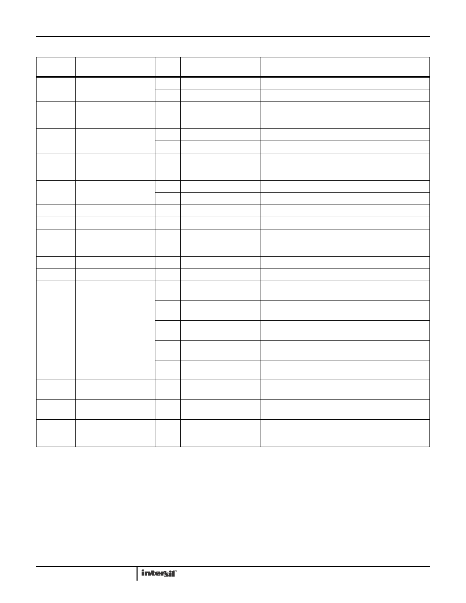
0x19
Red Offset LSB, (0x00)
5:0
N/A
7:6
Red Offset LSB
2 LSBs of 10-bit offset word
0x1A
Green Offset MSB, (0x80)
7:0
Green Offset MSB
ABLC off: upper 8-bits to Green offset DAC
ABLC enabled: Green digital offset
(See Red Offset)
0x1B
Green Offset LSB, (0x00)
5:0
N/A
7:6
Green Offset LSB
See Red Offset
0x1C
Blue Offset MSB, (0x80)
7:0
Blue Offset MSB
ABLC off: upper 8-bits to Blue offset DAC
ABLC enabled: Blue digital offset
(See Red Offset)
0x1D
Blue Offset LSB, (0x00)
5:0
N/A
7:6
Blue Offset LSB
See Red Offset
0x1E
PLL Htotal MSB, (0x06)
5:0
PLL Htotal MSB
14-bit HTOTAL. PLL updated on LSB write only.
0x1F
PLL Htotal LSB, (0x98)
7:0
PLL Htotal LSB
PLL updated on LSB write only. SXGA default
0x20
PLL Phase, (0x00)
5:0
PLL Sampling Phase
Used to control the phase of the ADC’s sample point relative
to the period of a pixel. Adjust to obtain optimum image quality.
One step = 5.625° (1.56% of pixel period).
0x21
PLL Pre-coast, (0x04)
7:0
Pre-coast
Number of lines the PLL will coast prior to the start of VSYNC.
0x22
PLL Post-coast, (0x04)
7:0
Post-coast
Number of lines the PLL will coast after the end of VSYNC.
0x23
PLL Misc, (0x00)
0
PLL Lock Edge HSYNC
0: PLL locks to trailing edge of selected HSYNC (default)
1: PLL locks to leading edge of selected HSYNC
1
CLKINV ENABLE
0: CLKINV input ignored
1: CLKINV input enabled
2
Ext Coast SEL
0: Internal COAST generation
1: External COAST source
3
Ext Coast POL
0: Active high external COAST
1: Active low external COAST
4
EXT CLOCK
0: Internal pixel clock from DPLL
1: External pixel clock from EXTCLKin pin
0x24
DC Restore and ABLC
starting pixel MSB, (0x00)
5:0
DC Restore and ABLC
starting pixel (MSB)
Pixel after Raw HSYNC trailing edge to begin DC restore and
ABLC. 14-bits.
0x25
DC Restore and ABLC
starting pixel LSB, (0x02)
7:0
DC Restore and ABLC
starting pixel (LSB)
0x26
DC Restore Clamp Width,
(0x10)
7:0
DC Restore clamp width
Only applies to DC restore clamp used for AC-coupled
configurations. A value of 0x00 means the clamp DAC is never
connected to the input.
Register Listing (Continued)
ADDRESS
REGISTER
(DEFAULT VALUE)
BITS
FUNCTION NAME
DESCRIPTION
ISL51002
发布紧急采购,3分钟左右您将得到回复。
相关PDF资料
ISL5314IN
IC SYNTHESIZER DIGITAL 48-MQFP
ISL55100AIRZ-T
IC COMP DRVR/WINDOW 18V 72-QFN
ISL55100BIRZ
IC COMP DRVR/WINDOW 18V 72-QFN
ISL5627INZ
IC DAC DUAL 8BIT 3.3V 48-LQFP
ISL5629/2INZ
IC DAC 8BIT CMOS DUAL 48LQFP
ISL5727INZ
IC DAC DUAL 10BIT 3.3V 48-LQFP
ISL5729/2INZ
IC DAC 10BIT CMOS DUAL 48LQFP
ISL5757IBZ
IC DAC 10BIT 260MHZ 28-SOIC
相关代理商/技术参数
ISL51002CQZ-150
制造商:Intersil Corporation 功能描述:AFE VID 3ADC 10-BIT 1.8V/3.3V 128MQFP EP - Trays 制造商:Intersil 功能描述:10 BIT VID AFE MEASURE&AUTO-ADJUST 制造商:Intersil Corporation 功能描述:10-Bit Video Analog Front End (AFE) with Measurement and Auto-Adjust Features
ISL51002CQZ-165
功能描述:IC FRONT END 10BIT VID 128-MQFP RoHS:是 类别:集成电路 (IC) >> 数据采集 - 模拟前端 (AFE) 系列:- 产品培训模块:Lead (SnPb) Finish for COTS
Obsolescence Mitigation Program 标准包装:2,500 系列:- 位数:- 通道数:2 功率(瓦特):- 电压 - 电源,模拟:3 V ~ 3.6 V 电压 - 电源,数字:3 V ~ 3.6 V 封装/外壳:32-VFQFN 裸露焊盘 供应商设备封装:32-QFN(5x5) 包装:带卷 (TR)
ISL51002EVALZ
制造商:INTERSIL 制造商全称:Intersil Corporation 功能描述:10-Bit Video Analog Front End (AFE) with Measurement and Auto-Adjust Features
ISL51002-EVALZ
功能描述:EVAL BOARD FOR ISL51002 RoHS:是 类别:编程器,开发系统 >> 评估演示板和套件 系列:* 产品培训模块:Obsolescence Mitigation Program 标准包装:1 系列:- 主要目的:电源管理,电池充电器 嵌入式:否 已用 IC / 零件:MAX8903A 主要属性:1 芯锂离子电池 次要属性:状态 LED 已供物品:板
ISL5100A
制造商:INTERSIL 制造商全称:Intersil Corporation 功能描述:Quad 18V Pin Electronics Driver/Window Comparator
ISL5101IB
制造商:Intersil Corporation 功能描述:
ISL5120
制造商:INTERSIL 制造商全称:Intersil Corporation 功能描述:Low-Voltage, Single Supply, Dual SPST, SPDT Analog Switches
ISL5120CB
功能描述:IC SWITCH DUAL SPST 8SOIC RoHS:否 类别:集成电路 (IC) >> 接口 - 模拟开关,多路复用器,多路分解器 系列:- 标准包装:48 系列:- 功能:开关 电路:4 x SPST - NO 导通状态电阻:100 欧姆 电压电源:单/双电源 电压 - 电源,单路/双路(±):2 V ~ 12 V,±2 V ~ 6 V 电流 - 电源:50nA 工作温度:-40°C ~ 85°C 安装类型:表面贴装 封装/外壳:16-SOIC(0.154",3.90mm 宽) 供应商设备封装:16-SOIC 包装:管件